


The field of oxide thin-film transistors (TFTs)is very broad as it includes any TFT employing an oxide semiconductor material as its active layer. At ADRC, based on the deposition method of the oxide semiconductor, two groups of oxide TFTs are studied: (1) Oxide TFTs by sputtering) and (2) Oxide TFTs by solution process. Although the first group involves other sputtered oxide semiconductors such as indium-zinc-oxide (IZO), amorphous-indium-gallium-zinc-oxide (a-IGZO) is major oxide semiconductor studied. In the second group, a number of solution processed oxide semiconductors, including zinc tin oxide (ZTO), indium-zinc-tin-oxide (IZTO), zinc-oxide (ZnO), indium oxide (InOX), and tin-zinc-oxide (SnZnO) are being studied as active materials..
- 1) a-IGZO TFT
- a) Device Structure
At ADRC, several device structures are employed for a-IGZO TFTs, including the ones shown in Figure 1. Basically, all metal electrodes are sputtered Mo. However, for dielectrics, plasma-enhanced chemical vapor deposited SiO2 or SiOX has to be used for good device performance and stability [1]-[8].
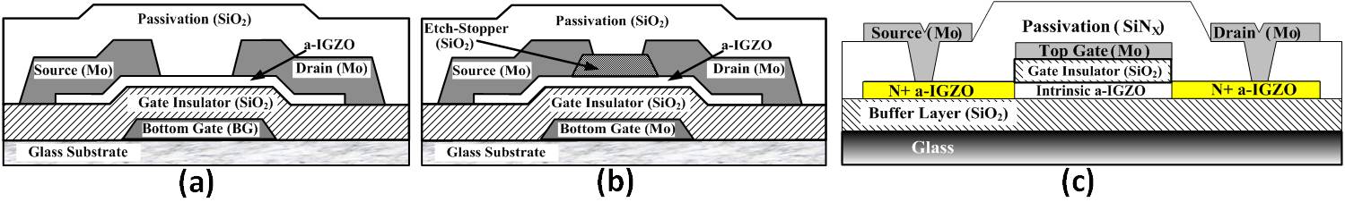
Figure 1. a-IGZO TFT structures: a) Back channel etched (BCE). b) Etch stopper, and c) Coplanar
[1] S. H. Park, et al., Appl. Phys. Lett., 103, 043509 (2013).
[2] D. H. Kang, et al., Appl. Phys. Lett. 102, 083508 (2013).
[3] M. Mativenga, et al., AIP Advances, 2, 032129 (2012).
[4] D. Geng, et al., IEEE Electron Device Lett., 33, 1012 (2012).
[5] M. Mativenga, et al., Solid State Commun., 152, 1739 (2012).
[6] S. H. Ryu, et al., ECS Solid State Lett., 1 Q17(2012).
[7] U. G. Lee, et al., IEEE Electron Device Lett., 33, 812 (2012).
[8] M. Mativenga, et al., IEEE Electron Device Lett., 33, 824 (2012).
b) TFT operation
The a-IGZO TFTs fabricated at ADRC are among the best worldwide, exhibiting good on state characteristics with large field-effect mobility, small sub-threshold gate voltage swing, and small sub-threshold voltage as shown in Figure 2 [9].
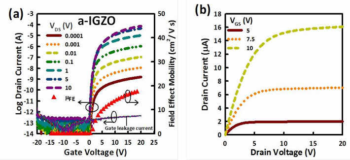
Figure 2. Operation of an a-IGZO TFT with an etch stopper structure:
a) Transfer characteristics. b) Output characteristics
[9] M. Mativenga, et. al., IEEE Trans. Electron Devices, 59, 2501(2012).
c) Stability
Research goals at ADRC include the optimization of the fabrication process and device structure for high electrical and environmental stability over long periods of time and under harsh conditions. Therefore, research aimed at understanding the device physics governing oxide TFTs is being done at ADRC. Particularly, electrical instabilities of oxide TFTs under various conditions, including positive-bias-stress (PBS), negative-bias-stress (NBS), negative-bias-under-illumination-stress (NBIS), positive-bias-and-temperature-stress (PBTS), and high-current-stress (HCS) are being researched [10-14]. Figures 3 and 4 show the mechanisms of PBS and NBIS, respectively.
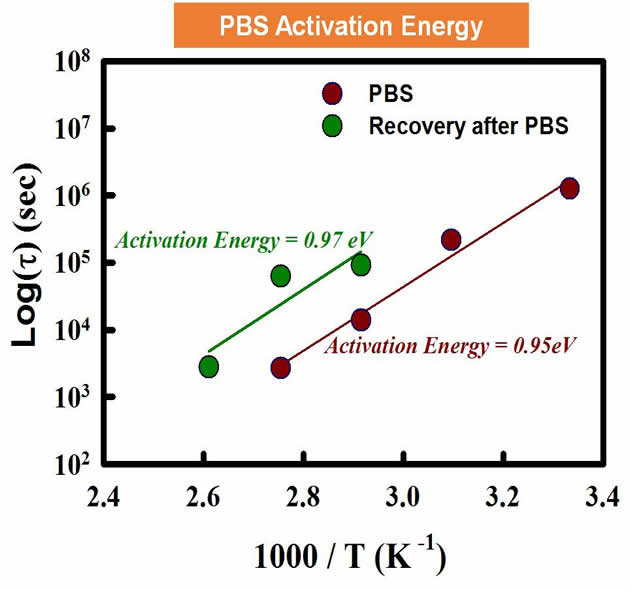
Figure 3. Positive bias stress (PBS) activation energy. Equal activation energies for stress and recovery indicate that carrier migration plays a great role under positive bias stress in a-IGZO TFTs [10].
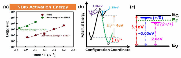
Figure 4. Mechanism of negative bias and illumination stress (NBIS).
(a) Activation energy [10].
(b) Proposed configuration coordinate diagram for creation and recovery of NBIS defects. The relevant crystal states are labeled as: ‘A’, ground state; ‘B’, saddle point; ‘C’, neutral oxygen vacancy state; ‘D’, doubly ionized oxygen vacancy state; ‘E’, weak or reconstructed bond state. As explained in Ref. [11], the associated energies are as follows: E(B)-E(A)=5.25eV; E(C)-E(A)=4eV=Hf0, neutral vacancy formation energy; E(D)-E(A)= Hf++ <0, formation energy of the doubly ionized vacancy; E(B)-E(E)=1.06eV, activation energy for NBIS; E(B)-E(C)=1.25eV, activation energy for NBIS recovery [11], [12].
(c) Positive corelelation energy (+ U) behaviour in a-IGZO [11].
- 2) Oxide TFTs by Solution Process
- a) Fabrication Process
In solution processed oxide TFTs, either/both the gate-insulator (GI) or/and active oxide semiconductor are solution processed. The solutions are prepared by mixing precursor solutions of the respective oxide materials with a solvent. The solution is then deposited onto the sample either by spin coating or ink-jet printing. This section only describes the spin coated oxides. Please refer to the following “Inkjet Printed” section for printed oxides. Solution processed gate-insulators include yttrium oxide (YOX), aluminum oxide (AlOX), hafnium-oxide (HfOX), zirconium oxide (ZrOX) e.t.c. As mentioned in the introduction, solution processed oxide semiconductors include ZTO, IZTO, ZnO, InOX, and SnZnO. Figure 4 below show an example of the fabrication process of an InOX TFT. The gate insulator is solution processed AlOX (solvent: Acetonitrile/ Ethylene-glycol; precursor: AlCl3) and the active layer is solution processed InOX (solvent: Acetonitrile/ Ethylene-glycol; precursor: InCl3). Compared to sputtering or PECVD, spin coating is simpler, cheaper, and easier to maintain.
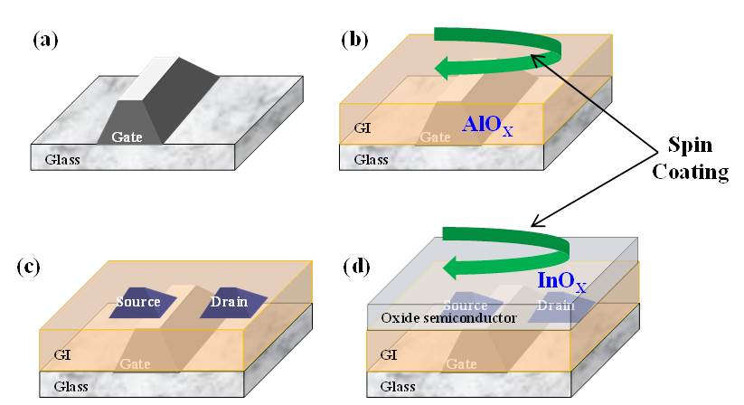
Figure 5. Fabrication process flow of a spin coated InOX TFT.
[1] C. Avis et al., J. Mater. Chem., 22, 17415(2012)
[2] Y. G. Kim et al.,ECS Solid State Lett., 1, Q23(2012)
[3] C. Avis and J. Jang, Jpn. J. Appl. Phys., 50, 01BG03(2011)


