


Low-temperature polycrystalline silicon (LTPS) is of increasing interest for largearea electronics such as active-matrix
liquid-crystal displays (AMLCDs) and active matrix organic light emitting diodes (AMOLEDs) because of its high
field-effect mobility compared to amorphous silicon.
Especially, Ni mediated crystallization of
a-Si was studied a lot because of its simple and low temperature process for poly-Si. However, in conventional MIC
(metal induced crystallization) or MILC (metal induced lateral crystallization), the metal layer for inducing crystallization was deposited
at least on a portion of a-Si surface. In this case, the Ni-contacted region on the a-Si for metal-induced crystallization can be contaminated
by Ni. To achieve a metal induced crystallization of a-Si using a cap layer (MICC) with clean and smooth surface, we developed
a technique to make poly-Si with large grain by thermal annealing.
Fig. The optical microscopy images of selectively Secco-etched poly-Si films. The samples were crystallized at 580 ¡ÆC for 30 min (a), 1 h (b), 2 h (c), and 20 h (d).
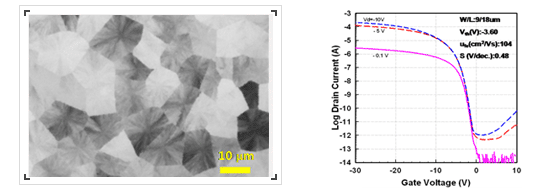
Fig. The optical microscopy image of grain and transfer characteristics of MICC poly-Si TFTs
Conventional excimer laser crystallization (ELC), which uses overlap scanning with a line beam, is acknowledged as a useful technique to form poly-Si films on large glass substrates with a high throughput. The grains are nearly single crystalline but the size of the grains are less than one micrometer. It is generally believed that the formation of large grains is beneficial to achieving high field-effect mobility.
Continuous wave (CW) laser crystallization also seems useful in forming high-quality Si films with very large grains. The poly-Si film by CW laser
annealing shows various microstructures from very small grains with average size of several tens of nanometers to large grains over 10 μm. This can be achieved by optimizing the crystallization conditions such as the laser power and the scanning speed. The TFT on the SLC region shows good electrical performance.
[Y.D. Son, N.K. Son, K.H. Kim, E.H. Kim, J.H. Oh and J. Jang, Society for Information Display 2007, (2007) pp. 76]


